


Please Leave Us A Message
Privacy statement: Your privacy is very important to Us. Our company promises not to disclose your personal information to any external company with out your explicit permission.

Shenzhenshi Zhenhuan Electronic Co., Ltd
 November 28, 2019
This article briefly describes how to use ST's secondary side device TSM family to reduce the no-load power consumption of chargers and power adaptor. This family has precise voltage and current regulation, and can make the whole system under no load conditions under no load conditions. The total power consumption is reduced to nearly 100mW.
The TSM101x family integrates a voltage reference device and two operational amplifiers and is a highly integrated switching power supply solution that requires constant voltage (CV) and constant current (CC) modes. The integration of a voltage reference device and an operational amplifier makes it an ideal voltage controller. Another op amp, in conjunction with this integrated voltage reference device and several external resistors, functions as a current limiter.
These products are used in Battery Charger and ac dc adapter that require constant voltage and output current limiting and can be used in a wide range of applications with voltage reference accuracy between 0.5% and 1%.
In a typical charger and adapter system, different factors increase total power consumption without load. However, in terms of breadth, the total power consumption can be divided into power consumption (Pout) generated on the secondary side and power consumption (Pin) generated on the primary side.
Secondary side power consumption
This article focuses on how to reduce the secondary side power consumption, so we start from the typical circuit diagram of the secondary side of the switching Power Supply application, see Figure 1 below.
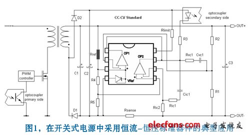
The constant current-constant voltage standard device is a monolithic integrated circuit that integrates two operational amplifiers. Of the two op amps, one is a separate device and the other non-inverting input is connected to a 2.5V fixed voltage reference circuit. ST's TSM103W is a typical application for such secondary side devices.
Constant current-constant voltage devices are usually parallel circuits, which means that the internal current generator requires an external power supply to polarize and fix the reference voltage at 2.5V (Vref = 2.5V).
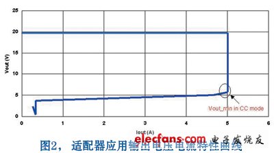
If we assume that Vout is connected to a dead battery, we will see the output voltage-current characteristic of Figure 2.
From Figure 2, we can easily see that the load uses a gradual charging method, first increasing the current, and then increasing the voltage so that the voltage drop reaches a minimum. This gradual charging method ensures that the current is limited and a stable current is achieved. Thereafter, the voltage begins to rise (while the current remains constant) until a constant voltage value.
In a typical adapter application, the maximum output voltage is 20V (without load) and the minimum output voltage is 5V (the minimum voltage value for maintaining constant current).
In order to maintain Vout_min = 5V, Vcc_min = 5V, the minimum current value required to bias Vref is 1mA, which means: ![]()
Therefore, in order to maintain Vout_min = 5V, we must fix the reference resistance at Rref = 2.5k
Since we have fixed the reference resistor Rref, we should consider the no-load condition of Vout_max = 20V. According to the formula below: 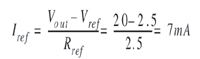
The total power consumption of the secondary side is calculated by the following formula: Pout = Vout Vtot
Where Itot = Icc + Iref + Iopto
Moreover, the current Iopto required to drive an optocoupler is typically 1.5 mA.
This shows that for a no-load typical system with Vout = 20V, Iref = 7mA, Icc = 1.5mA, Iopto = 1.5mA, the secondary side power dissipation (Pout) is equal to:
Pout = (Vout Vtot) = (Vtot (Iref + Icc + Iopto)) = (20V (7mA + 1.5mA + 1.5mA)) = (20V 10mA) = 200mW
Primary side power consumption
Now we turn our attention to the primary side of a typical adapter application. The primary side of a switching power supply consists of several functional blocks (eg, power factor correction and pulse width modulation), each of which increases the total power consumption of the device. However, the total power dissipation due to the primary side function block is typically assumed to be around 80mW under no load conditions (because the power range of the charger and adapter is within 5W).
The rated power is a key factor in the overall power consumption of the primary side, with a maximum rated power of approximately 50%. That is to say, 1 mW of power is transmitted to the secondary side, and 2 mW of power is required on the primary side.
Back to our equation calculation above, under no-load conditions, if we need 200mW of power on the secondary side, we must generate 400mW of power on the primary side, and we need 80mW of current to drive the pulse width modulation controller.
This relationship shows that if the no-load power consumption is reduced on the secondary side, then the primary side will receive twice the benefit.
The above is the Reduce the total power consumption of chargers and adapters without load we have listed for you. You can submit the following form to obtain more industry information we provide for you.
You can visit our website or contact us, and we will provide the latest consultation and solutions
Send Inquiry
Most Popular
lastest New
Send Inquiry
Privacy statement: Your privacy is very important to Us. Our company promises not to disclose your personal information to any external company with out your explicit permission.
Fill in more information so that we can get in touch with you faster
Privacy statement: Your privacy is very important to Us. Our company promises not to disclose your personal information to any external company with out your explicit permission.