


Please Leave Us A Message
Privacy statement: Your privacy is very important to Us. Our company promises not to disclose your personal information to any external company with out your explicit permission.

Shenzhenshi Zhenhuan Electronic Co., Ltd
 January 03, 2020
Is there no failure of the CBB capacitor?
Tip 1: Use an LDO regulator to power a 3.3V system from a 5V supply
The voltage differential across a standard three-terminal linear regulator is typically 2.0-3.0V. To reliably convert 5V to 3.3V, you cannot use them. Drop Dropout (LDO) regulators with a dropout voltage of a few hundred millivolts are ideal for this type of application. Figure 1-1 is a block diagram of a basic LDO system with corresponding currents. As can be seen from the figure, LDO consists of four major components:
Turn on transistor
2. Bandgap reference source
3. Operational Amplifier
4. Feedback resistor divider
When choosing an LDO, it is important to know how to distinguish the various LDOs. The device's quiescent current, package size, and model are important device parameters. According to the specific application to determine various parameters, the optimal design will be obtained.
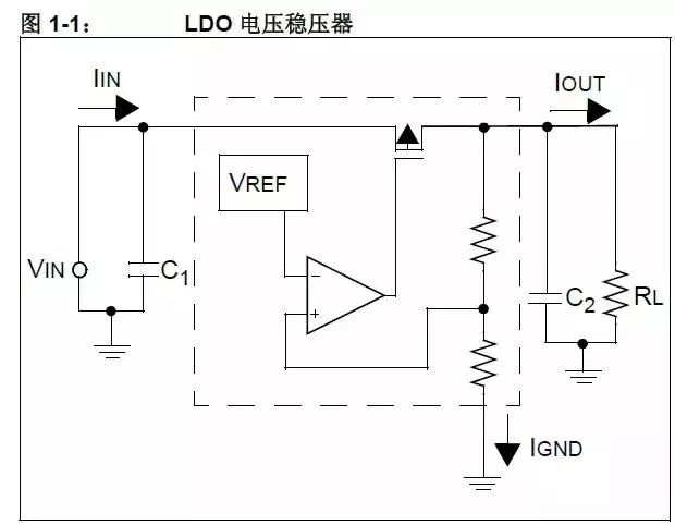
The quiescent current IQ of the LDO is the device's ground current, IGND, when the device is operating with no load. IGND is the current that the LDO uses to regulate. When IOUT>>IQ, the efficiency of the LDO can be approximated by dividing the output voltage by the input voltage. However, at light loads, IQ must be included in the efficiency calculation. LDOs with lower IQ have higher light load efficiency. The increase in light-load efficiency has a negative impact on LDO performance. Higher quiescent current LDOs have a faster response to sudden changes in line and load.
Tip 2: Low Cost Power Supply System Using Zener Diodes
A detailed description of a low-cost regulator scheme using Zener diodes is provided here.
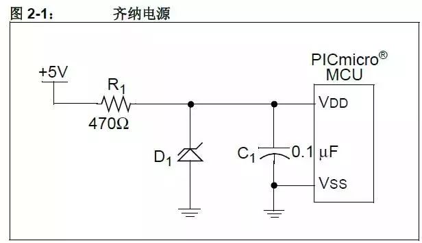
A simple, low-cost, 3.3V regulator can be made with Zener diodes and resistors, as shown in Figure 2-1. In many applications, this circuit can replace LDO regulators and is cost-effective. However, this regulator is more sensitive to load than LDO regulators. In addition, it is less energy efficient because R1 and D1 always have power consumption. R1 limits the current flowing into D1 and PICmicro® MCUs to keep VDD within the allowable range. As the current flowing through the zener diode changes, the reverse voltage of the diode will also change, so we need to carefully consider the value of R1.
R1 is selected on the basis that at a maximum load, usually when the PICmicro MCU is running and its output is driven high, the voltage drop across R1 is low enough to allow the PICmicro MCU to have sufficient voltage to maintain operation. At the same time, at the minimum load, usually when the PICmicro MCU is reset, VDD does not exceed the zener diode's rated power and does not exceed the PICmicro MCU's maximum VDD.
Tip 3: A Lower-Cost Power Supply System Using Three Rectifier Diodes
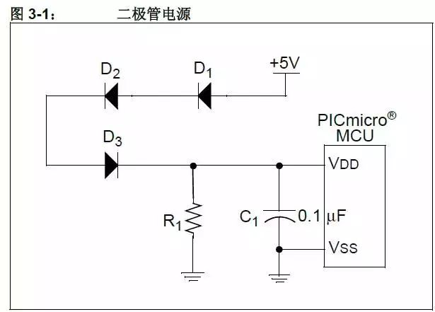
Figure 3-1 details a lower-cost regulator solution using three rectifier diodes.
We can also connect several conventional switching diodes in series and use their forward voltage drop to reduce the voltage of the incoming PICmicro MCU. This is even lower than the cost of a Zener diode regulator. The current consumption of this design is usually lower than that of a circuit using a Zener diode.
The number of diodes required varies depending on the forward voltage of the selected diode. The voltage drop of diodes D1-D3 is a function of the current flowing through these diodes. Connection R1 is to avoid that the voltage on the PICmicro MCU VDD pin exceeds the maximum VDD value of the PICmicro MCU when the load is minimal—usually when the PICmicro MCU is in reset or in hibernation. Depending on other circuits connected to VDD, the resistance of R1 can be increased or even R1 may not be needed at all. Diodes D1-D3 are selected based on the following: At a maximum load, typically when the PICmicro MCU is running and driving its output high, the voltage drop across D1-D3 is low enough to meet the PICmicro MCU's minimum VDD requirement.
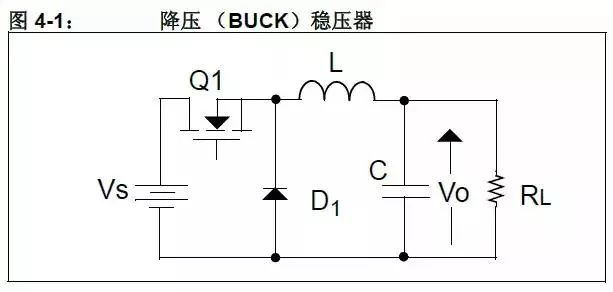
Tip 4: Use a Switching Regulator to Power a 3.3V System from a 5V Supply
As shown in Figure 4-1, a buck switching regulator is an inductor-based converter that reduces the input voltage source to a lower amplitude output voltage. Output regulation is achieved by controlling the ON time of MOSFET Q1. Since the MOSFET is either in a low-impedance state or in a high-impedance state (ON and OFF, respectively), a high input source voltage can be efficiently converted to a lower output voltage.
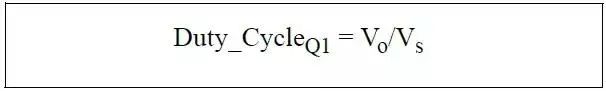
When Q1 is in these two states, the relationship between the input and output voltage can be established by balancing the voltage-time of the inductor.

For MOSFET Q1, there is the following equation:
When selecting the value of the inductor, it is a good initial choice to make the maximum peak-to-peak ripple current of the inductor equal to 10% of the maximum load current.

When selecting the output capacitor value, a good initial value is: make the characteristic impedance of the LC filter equal to the load resistance. In this way, if the load is suddenly removed during full load operation, the voltage overshoot can be within an acceptable range.

When selecting diode D1, select a component with a large enough current rating to be able to withstand the inductor current during pulse period (IL) discharge.
Digital connection
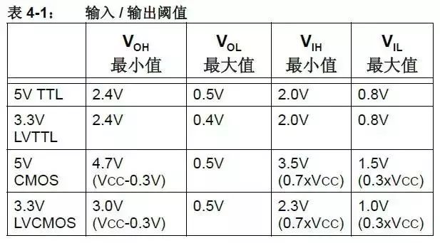
When connecting two devices with different operating voltages, their respective output and input thresholds must be known. After knowing the threshold, the device connection method can be selected based on other application requirements. Table 4-1 shows the output and input thresholds used in this document. When designing the connection, be sure to refer to the manufacturer's data sheet to obtain the actual threshold level.
Tip Five: 3.3V → 5V Direct Connection
The simplest and most ideal way to connect a 3.3V output to a 5V input is direct connection. Direct connection needs to meet the following 2 requirements:
• VOH at 3.3V output is greater than VIH at 5V input
• 3.3V output VOL is less than 5V input VIL
One of the examples that can use this method is to connect the 3.3V LVCMOS output to the 5V TTL input. From the values given in Table 4-1, it can be clearly seen that all the above requirements are satisfied.
3.3V LVCMOS VOH (3.0V) greater than 5V TTL VIH (2.0V)
And
3.3V LVCMOS VOL (0.5V) is less than 5V TTL VIL (0.8V).
If these two requirements are not met, additional circuitry is required to connect the two parts. For possible solutions, see tips 6, 7, 8 and 13.
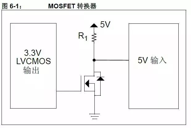
Tip 6: Use 3.3V → 5V MOSFET Converter
If the VIH of a 5V input is higher than the VOH of a 3.3V CMOS device, additional circuitry is required to drive any such 5V input. Figure 6-1 shows a low-cost, two-element solution.
When selecting the value of R1, two parameters need to be considered: the input switching speed and the current consumption on R1. When switching the input from 0 to 1, the input rise time due to the RC time constant formed by R1, the input capacitance of the 5V input, and any stray capacitance on the board must be taken into account. The input switching speed can be calculated by the following formula:

Since the input capacitance and the stray capacitance on the board are fixed, the only way to increase the input switching speed is to reduce the value of R1. Lowering the R1 resistance for faster switching time is at the expense of increasing the current consumption when the 5V input is low. In general, switching to 0 is much faster than switching to 1, because the on-resistance of an N-channel MOSFET is much less than R1. In addition, when selecting an N-channel FET, the VGS of the selected FET should be lower than the VOH of the 3.3V output.
Tip 7: Using 3.3V → 5V Diode Compensation
Table 7-1 lists the 5V CMOS input voltage thresholds, 3.3V LVTTL, and LVCMOS output drive voltages.

From the above table, the high and low input voltage thresholds of the 5V CMOS input are all about one volt higher than the threshold of the 3.3V output. Therefore, even if the output from the 3.3V system can be compensated, there is little or no room left for noise or component tolerances. What we need is a circuit that can compensate for the output and increase the high and low output voltage difference.
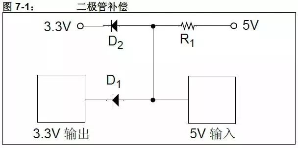
After the output voltage specification is determined, it has been assumed that the high output drives the load between the output and ground, while the low output drives the load between 3.3V and the output. If the load of the high voltage threshold is actually between the output and 3.3V, the output voltage is actually much higher because the mechanism for pulling the output high is the load resistance, not the output transistor.
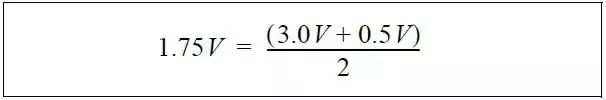
If we design a diode compensation circuit (see Figure 7-1), the forward voltage (typically 0.7V) of diode D1 will cause the output low voltage to rise, resulting in a low voltage of 1.1V to 1.2V at the 5V CMOS input. It is safely below the low input voltage threshold of the 5V CMOS input. The high output voltage is determined by the pull-up resistor and diode D2 connected to the 3.3V supply. This makes the output high voltage approximately 0.7V higher than the 3.3V supply, ie, 4.0 to 4.1V, which is safe above the 5V CMOS input threshold (3.5V).
Note: In order for the circuit to function properly, the pull-up resistor must be significantly smaller than the input resistance of the 5V CMOS input to avoid the output voltage drop due to the input resistor divider effect. The pull-up resistor must also be large enough to ensure that the current loaded on the 3.3V output is within device specifications.
Tip eight: 3.3V → 5V voltage comparator
The basic work of the comparator is as follows:
• When the inverting (-) input voltage is greater than the in-phase (+) input voltage, the comparator output switches to Vss.
• Comparator output is high when the in-phase (+) input voltage is greater than the inverting (-) input voltage.
In order to maintain the polarity of the 3.3V output, the 3.3V output must be connected to the non-inverting input of the comparator. The comparator's inverting input is connected to the reference voltage defined by R1 and R2, as shown in Figure 8-1.

Calculate R1 and R2
The ratio of R1 to R2 depends on the logic level of the input signal. For a 3.3V output, the inverting voltage should be placed at the midpoint voltage between VOL and VOH. For LVCMOS output, the midpoint voltage is:
If the logic levels of R1 and R2 are as follows,
If R2 is 1K, R1 is 1.8K.
A properly connected op amp can be used as a comparator to convert a 3.3V input signal to a 5V output signal. This is due to the use of the comparator's characteristic that the comparator forces the output to a high (VDD) or low (Vss) level based on the magnitude of the voltage differential between the "inverting" input and the "in-phase" input.
Note: The output must have rail-to-rail drive capability for the op amp to operate properly at 5V.

Tip nine: 5V → 3.3V direct connection
The 5V output typically has a VOH of 4.7 volts and a VOL of 0.4 volts; whereas a 3.3-V LVCMOS input typically has a VIH of 0.7 x VDD and a VIL of 0.2 x VDD.
There is no problem when the 5V output drive is low because the 0.4 volt output is less than the 0.8 volt input threshold. When the 5V output is high, the 4.7V VOH is greater than 2.1V VIH, so we can directly connect the two pins without conflict, provided the 3.3V CMOS output can tolerate 5V.
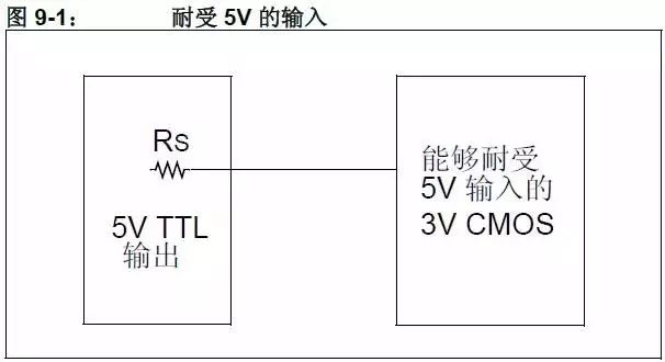
If the 3.3V CMOS input does not tolerate 5 volts, a problem occurs because the input's maximum voltage specification is exceeded. For possible solutions, see Tips 10-13.
Tip 10: Use 5V → 3.3V Diode Clamp
Many vendors use clamp diodes to protect the device's I/O pins and prevent the voltage on the pins from exceeding the maximum allowable voltage specification. The clamping diodes cause the voltage on the pins to fall no more than one diode drop below Vss and no more than one diode drop above VDD. To use a clamp diode to protect the input, still pay attention to the current flowing through the clamp diode. The current flowing through the clamp diode should always be small (on the microampere level). If the current through the clamp diode is too high, there is a danger of the parts blocking. Since the source resistance of the 5V output is usually around 10Ω, a series resistor is still needed to limit the current flowing through the clamping diode, as shown in Figure 10-1. The consequence of using a series resistor is to reduce the speed of the input switch because the RC time constant is formed on the pin (CL).
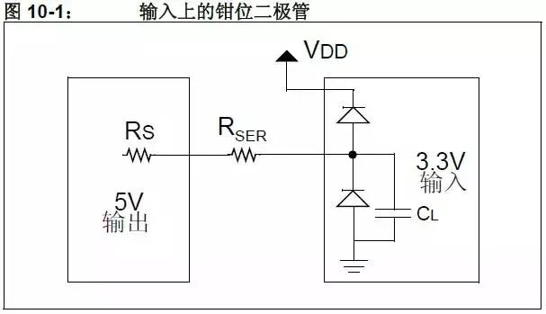
If there is no clamping diode, an external diode can be added to the current, as shown in Figure 10-2.

Tip 10: A 5V → 3.3V Active Clamp
One problem with diode clamping is that it will inject current into the 3.3V supply. In designs with a high-current 5V output and a light-load 3.3V rail, this current injection may cause the 3.3V supply voltage to exceed 3.3V. To avoid this problem, a triode can be used instead. The triode allows excess output drive current to flow to ground instead of the 3.3V supply. The designed circuit is shown in Figure 11-1.

The base-emitter junction of Q1 plays the same role as the diode in the diode clamp circuit. The difference is that only a few percent of the emitter current flows out of the base into the 3.3V rail, and most of the current flows to the collector and harmlessly flows into the ground from the collector. The ratio of the base current to the collector current, which is determined by the current gain of the transistor, is usually 10-400, depending on the transistor used.
Tip 12: 5V → 3.3V Resistor Divider
A simple resistor divider can be used to reduce the output of a 5V device to a level suitable for a 3.3V device input. The equivalent circuit of this interface is shown in Figure 12-1.

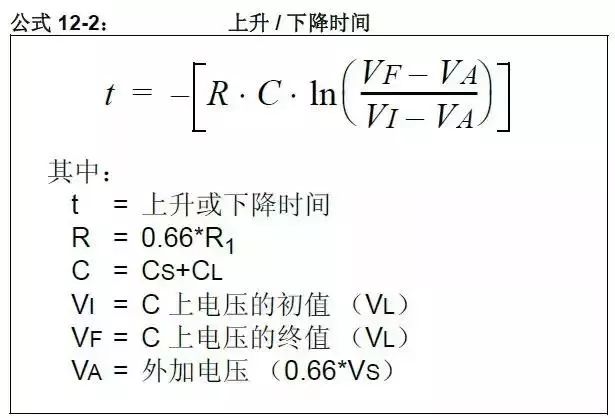
In general, the source resistance RS is very small (less than 10Ω). If the selected R1 is much larger than the RS, then the impact of RS on R1 can be ignored. At the receiving end, the load resistance RL is very large (greater than 500 kΩ). If the selected R2 is much smaller than RL, the effect of RL on R2 can be ignored.
There is a trade-off between power consumption and transient time. In order to minimize the power consumption of the interface current, the series resistors R1 and R2 should be as large as possible. However, the load capacitance (combined by the stray capacitance CS and the input capacitance CL of the 3.3V device) can adversely affect the rise and fall times of the input signal. If R1 and R2 are too large, the rise and fall times may be too long to be acceptable.
If the effects of RS and RL are ignored, the formula for determining R1 and R2 is given by Equation 12-1 below.

Equation 12-2 gives the formula for determining the rise and fall times. To facilitate circuit analysis, Thevenin equivalent calculations were used to determine the applied voltage VA and series resistance R. The Thevenin equivalent calculation is defined as the open circuit voltage divided by the short circuit current. According to the restrictions imposed by Equation 12-2, for the circuit shown in Figure 12-1, the determined Thevenin equivalent resistance R should be 0.66*R1 and the Thevenin equivalent voltage VA should be 0.66*VS.
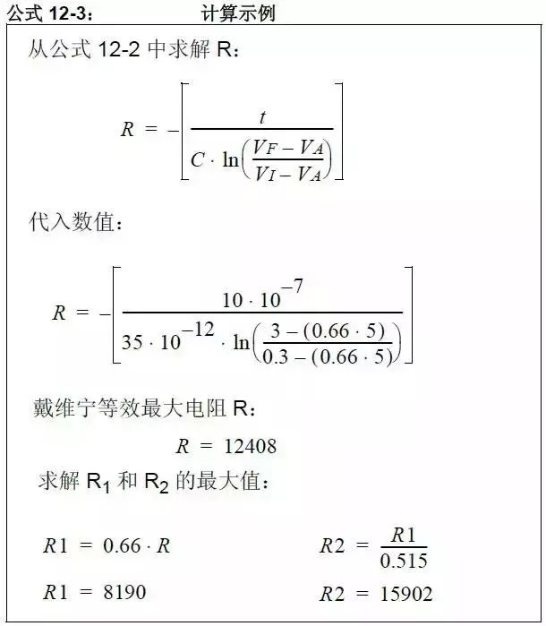
For example, suppose the following conditions exist:
• Stray capacitance = 30 pF
• Load capacitance = 5 pF
• Maximum rise time from 0.3V to 3V ≤ 1 μs
• Applied source voltage Vs = 5V
The calculation for determining the maximum resistance is shown in Equation 12-3.
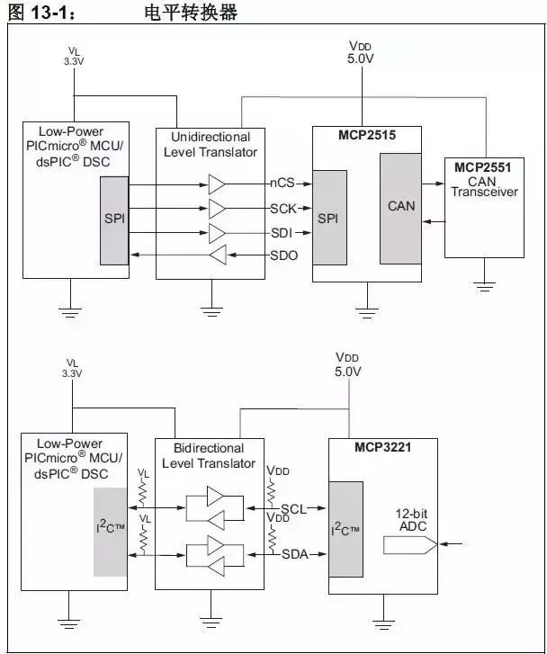
Tip 13: 3.3V → 5V Level Translator
Although level shifting can be done discretely, it is usually more popular to use an integrated solution. Level converters have a wide range of applications: one-way and two-way configurations, different voltage conversions, and different speeds for users to choose the best solution.
Board-level communication between devices (for example, MCU to peripherals) is done via SPI or I2CTM, which is the most common. For SPI, using a unidirectional level shifter is more appropriate; for I2C, a bidirectional solution is needed. Figure 13-1 below shows these two solutions.
simulation
The final challenge for a 3.3V to 5V interface is how to convert analog signals across power barriers. Low-level signals may not require external circuitry, but systems that transmit signals between 3.3V and 5V can be affected by power supply changes. For example, in a 3.3V system, the ADC converts a 1V peak analog signal with a higher resolution than the ADC conversion in a 5V system, because in the 3.3V ADC, more of the ADC's range is used for conversion. On the other hand, relatively high signal amplitudes in 3.3V systems may conflict with the lower common-mode voltage limitations of the system.
Therefore, in order to compensate for the above differences, some kind of interface circuit may be needed. This section will discuss the interface circuitry to help alleviate the problem of signal transitions between different power sources.
Tip 14: 3.3V→5V Analog Gain Block
When connecting from a 3.3V power supply to 5V, the analog voltage needs to be increased. The 33 kΩ and 17 kΩ resistors set the gain of the op amp so that full scale is used at both ends. The 11 kΩ resistor limits the current flowing back to the 3.3V circuit.

Tip 15: 3.3V→5V Analog Compensation Module
This module is used to compensate the 3.3V to 5V analog voltage. The following is the conversion of the analog voltage from the 3.3V supply to the 5V supply. The upper right 147 kΩ, 30.1 kΩ resistor, and +5V supply are equivalent to a 0.85V voltage source with a 25 kΩ resistor in series. This equivalent 25 kΩ resistor, three 25 kΩ resistors, and an op amp make up a differential amplifier with a gain of 1 V/V. The 0.85V equivalent voltage source will appear to shift any signal at the input upward by the same amplitude; the signal centered at 3.3V/2 = 1.65V will be centered around 5.0V/2 = 2.50V at the same time. The upper left resistor limits the current from the 5V circuit.

Sixteenth: 5V → 3.3V active analog attenuator
This technique uses an operational amplifier to attenuate the signal amplitude from a 5V to 3.3V system.
The easiest way to convert a 5V analog signal to a 3.3V analog signal is to use a resistor divider with an R1:R2 ratio of 1.7:3.3. However, there are some problems with this method.
1) The attenuator may be connected to a capacitive load and constitute an undesired low-pass filter.
2) The attenuator circuit may need to drive a low impedance load from a high impedance source.
In either case, an operational amplifier is needed to buffer the signal.
The required op amp circuit is the unity gain follower (see Figure 16-1).
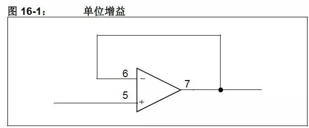
The output voltage of the circuit is the same as the voltage applied to the input.
In order to convert the 5V signal to a lower 3V signal, we simply add a resistor attenuator.

If the resistor divider is located before the unity-gain follower, it will provide the lowest impedance for the 3.3V circuit. In addition, the op amp can be powered from 3.3V, which will save some power. If the selected X is very large, the power consumption on the 5V side can be minimized.
If the attenuator is located after the unity gain follower, then there is the highest impedance for the 5V source. The op amp must be powered from 5V and the impedance on the 3V side will depend on the value of R1||R2.
Tip 17: 5V → 3.3V Analog Limiter
When transmitting a 5V signal to a 3.3V system, attenuation can sometimes be used as a gain. If the desired signal is less than 5V, then sending the signal directly to the 3.3V ADC will produce a large conversion value. There is danger when the signal is close to 5V. Therefore, there is a need for a method of controlling voltage over-limits without affecting the voltage in the normal range. Three implementation methods will be discussed here.
1. Use a diode to clamp the overvoltage to a 3.3V supply system.
2. Use Zener diodes to clamp the voltage to any desired voltage limit.
3. Use a diode-equipped op amp for accurate clamping.
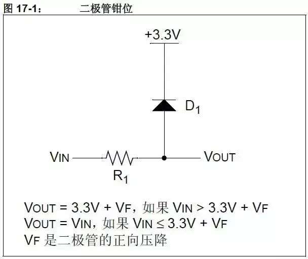
The simplest method of overvoltage clamping is the same as the simple method of connecting a 5V digital signal to a 3.3V digital signal. Use resistors and diodes to allow excess current to flow into the 3.3V supply. The resistor value chosen must be able to protect the diode and the 3.3V supply without negatively affecting the analog performance. If the impedance of the 3.3V supply is too low, this type of clamping may cause the 3.3V supply voltage to rise. Even if the 3.3V power supply has a very good low impedance, when the diode is turned on, and when the frequency is high enough, when the diode is not conducting (since there is a parasitic capacitance across the diode), such a clamp will make the input The signal is applying noise to the 3.3V power supply.
In order to prevent the input signal from affecting the power supply, or to make the input more responsive to large transient currents, a slight change has been made to the previous method and Zener diodes have been used instead. Zener diodes are usually slower than the fast signal diodes used in the first circuit. However, the Zener clamp is generally more robust and does not depend on the characteristics of the power supply when clamping. The size of the clamp depends on the current flowing through the diode. This is determined by the value of R1. If the output impedance of the VIN source is large enough, R1 may not be needed.

If you need a more accurate overvoltage clamp that does not depend on the power supply, you can use an op amp to get a precision diode. The circuit is shown in Figure 17-3. The op amp compensates for the forward voltage drop of the diode so that the voltage is clamped at the op amp's non-inverting input supply voltage. If the op amp is rail-to-rail, it can be powered with 3.3V.
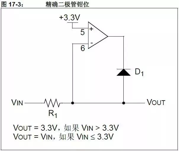
Since clamping is done through the op amp, it does not affect the power supply.
The op amp cannot improve the impedance that appears in the low-voltage circuit. The impedance is still R1 plus the source circuit impedance.
Tip Eighteen: Driving a Bipolar Transistor
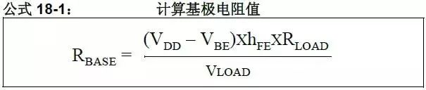
When driving a bipolar transistor, the base "drive" current and forward current gain (Β/hFE) will determine how much current the transistor will draw. If the transistor is driven by the microcontroller I/O port, use the port voltage and the upper limit of the port current (20 mA typical) to calculate the base drive current. If 3.3V technology is used, use a lower-resistance base current limiting resistor to ensure that there is sufficient base drive current to saturate the transistor.

The value of RBASE depends on the microcontroller power supply voltage. Equation 18-1 shows how to calculate RBASE.

If a bipolar transistor is used as a switch to turn on or off the load controlled by the microcontroller's I/O port pins, the smallest hFE specification and margin should be used to ensure that the device is fully saturated.
3V technology example:

For both of these examples, it is good practice to increase the base current margin. Driving 1mA base current to 2 mA ensures saturation, but at the cost of increased input power.
Tip 19: Drive N-Channel MOSFET Transistors
Care must be taken when selecting external N-channel MOSFETs for use with 3.3V microcontrollers. The MOSFET gate threshold voltage indicates the device's ability to fully saturate. For 3.3V applications, the rated MOSFET's rated on-resistance should be targeted for a gate drive voltage of 3V or less. For example, for a 100-mA load with a 3.3-V drive, a FET with a nominal drain current of 250 μA may not provide satisfactory results when applied with a 1-V gate-to-source voltage. When switching from 5V to 3V technology, carefully check the gate-to-source threshold and on-resistance characteristics as shown in Figure 19-1. Slightly reducing the gate drive voltage can significantly reduce the leakage current.

For MOSFETs, low-threshold devices are common and have a drain-to-source voltage rating of less than 30V. A MOSFET with a drain-to-source voltage rating greater than 30V typically has a higher threshold voltage (VT).

As shown in Table 19-1, the threshold voltage of this 30V N-Channel MOSFET switch is 0.6V. When the gate is applied with a voltage of 2.8V, the rated resistance of this MOSFET is 35mΩ, so it is very suitable for 3.3V applications.
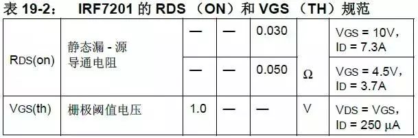
For the specifications in the IRF7201 data sheet, the minimum gate threshold voltage is specified as 1.0V. This does not mean that the device can be used to switch currents at a 1.0V gate-to-source voltage because there is no specification for VGS(th) below 4.5V. The IRF7201 is not recommended for 3.3V drive applications requiring low switching resistance, but it can be used for 5V drive applications.
Shenzhenshi Zhenhuan Electronic Co.,Ltd(www.szzhpower.com) was founded in 2008, specialize in external power adaptor, ac dc adapter, Outdoor Waterproof power supply, led driver, Power Transformer, switching power supply, dimmable or non-dimmable LED Drivers and Battery Charger in Shenzhen, China.
The above is the Is there no failure of the CBB capacitor? we have listed for you. You can submit the following form to obtain more industry information we provide for you.
You can visit our website or contact us, and we will provide the latest consultation and solutions
Send Inquiry
Most Popular
lastest New
Related Products
Send Inquiry
Privacy statement: Your privacy is very important to Us. Our company promises not to disclose your personal information to any external company with out your explicit permission.
Fill in more information so that we can get in touch with you faster
Privacy statement: Your privacy is very important to Us. Our company promises not to disclose your personal information to any external company with out your explicit permission.